
A PNP transistor is one of the two main types of bipolar junction transistors used in electronic circuits. It is a three-layer semiconductor device made up of two P-type layers with an N-type layer sandwiched between them. The three terminals of a PNP Transistor are called the Emitter, Base, and Collector.
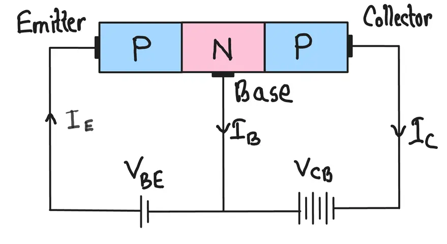
The image above shows the internal layout of a PNP transistor. The emitter and collector sections are made of P-type material and the base sits in between as N-type material.
Two voltage sources are shown in the diagram, \(V_{BE}\) across the emitter-base junction and \(V_{CB}\) across the collector-base junction. These voltages control how current moves through the device. The emitter current \(I_E\) flows out from the emitter, the base current \(I_B\) flows out from the base, and the collector current \(I_C\) flows into the collector.
In a PNP transistor, current flows from the emitter to the collector when a small current is drawn out of the base.
1. Structure and Symbol
The schematic symbol for a PNP transistor shows an arrow on the emitter pointing inward, toward the base.
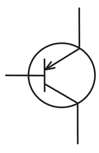
This diagram shows the standard symbol used for a PNP transistor in circuit schematics. The arrow on the emitter line points toward the base, which is the detail that separates a PNP symbol from an NPN symbol. In an NPN symbol, that same arrow points away from the base. This arrow direction is the easiest way to identify transistor type when reading a circuit diagram.
The three terminals connect to external circuitry:
- Emitter: This terminal supplies current carriers or holes into the base region. In a PNP transistor, the emitter is connected to the positive terminal of voltage supply.
- Base: Base is the control terminal of a PNP transistor. A small current pulled from the base controls a larger current flow between the emitter and collector.
- Collector: This terminal collects the current that flows through the transistor and connects to the load or the next stage of the circuit.
2. How a PNP Transistor Works
A PNP transistor conducts when the base is at a lower voltage than the emitter. This voltage difference must be at least 0.6 to 0.7 volts for silicon-based transistors.
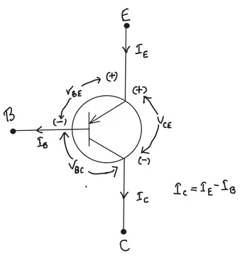
As shown in the above diagram \(I_E\) flows into the emitter terminal, \(I_B\) flows out from the base and \(I_C\) flows out from the collector. The polarity markings show that \(V_{BE}\) stays negative at the base side and the base sits at a lower voltage than the emitter during conduction.
The relationship between \(I_E\), \(I_B\) and \(I_C\) is given by:
\(\boxed{I_C=I_E – I_B}\)
The emitter-base junction acts like a PN junction diode. When this junction is forward biased or the emitter is more positive than the base by 0.6 to 0.7 volt threshold, current starts to flowing. Holes from the emitter move into the base, and most of these holes get pulled through to the collector due to the collector’s more negative voltage.
The base current controls the collector current and the relationship between them is described by the current gain, called beta \(\beta\) or \(h_{FE}\). If the beta value of a transistor is 100, then a base current of 1 mA can control a collector current of up to 100 mA.
3. Biasing a PNP Transistor
Biasing means setting up the DC voltages at each terminal so the transistor operates in the required region such as cutoff, active, or saturation region.
For a PNP transistor to conduct in the active region:
- The emitter must be at a higher voltage than the base (emitter-base junction is forward biased).
- The collector must be at a lower voltage than the base (base-collector junction is reverse biased).
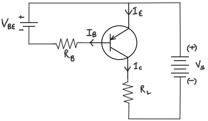
The above circuit diagram shows a biasing setup for a PNP transistor used as a switch. The \(V_{BE}\) source connects through the base resistor \(R_B\) to the base terminal, controlling the base current \(I_B\). On the collector side, the load resistor \(R_L\) connects to the supply voltage \(V_S\). The emitter connects directly to the top of the circuit, which ties back to the positive side of the supply.
Once \(V_{BE}\) forward biases the emitter-base junction, current starts flowing from \(I_E\) through the transistor and out through \(I_C\), passing through \(R_L\) to complete the circuit. This is a standard method for controlling a load using a PNP transistor.
4. PNP vs NPN Transistors
- Current Direction: In an NPN transistor, current flows into the base and out through the emitter. In a PNP transistor, current flows out of the base and into the emitter.
- Biasing Voltage: NPN transistors turn on when the base is more positive than the emitter. PNP transistors turn on when the base is more negative than the emitter.
- Common Use Case: NPN transistors are often used for low-side switching, where the transistor connects the load to ground. PNP transistors are used for high-side switching, where the transistor connects the load to the positive supply.
- Symbol Difference: The arrow on the emitter points outward for NPN and inward for PNP.
In practical terms, NPN transistors are more common in general-purpose circuits because they have better performance characteristics in terms of speed and gain. PNP transistors are necessary in specific applications in complementary pairs with NPN transistors for push-pull amplifier stages.
5. Practical Applications of PNP Transistors
High-Side Switching: PNP transistors are used to control the power side of a circuit. For example, if you want to switch a motor on and off, and the motor’s positive terminal connects to the power supply through the transistor, a PNP transistor makes more sense here. The transistor sits between the power source and the load, switching the connection based on the base signal.
Complementary Amplifier Circuits: Audio amplifiers commonly use a pair of NPN and PNP transistors together in a push-pull configuration. This allows the amplifier to handle both the positive and negative halves of an audio signal.
Current Sourcing: In some analog circuits, a PNP transistor supplies current to a load as a current source. This is useful in constant current circuits and some voltage regulator designs.
Relay Driver Circuits: PNP transistors are sometimes used to drive relays where the relay coil is connected to the positive supply and the transistor switches the ground-side connection based on a control signal.
6. Example Circuit: PNP Transistor as a Switch
Let’s walk through a simple example. Suppose you want to control an LED using a PNP transistor.
Connect the emitter of the PNP transistor to the positive supply, let’s say 5V as shown in the figure below. Connect the collector to one end of the LED, with the other end of the LED going through a resistor to ground. Connect the base to a resistor, and the other end of that resistor to a microcontroller pin.
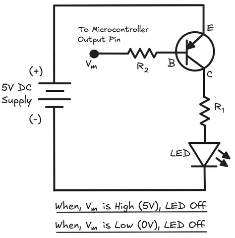
When the microcontroller pin outputs a high signal (5V), there is no voltage difference between the base and emitter, so the transistor stays off, and the LED remains off.
When the microcontroller pin outputs a low signal (0V), the base becomes more negative than the emitter, satisfying the 0.6 to 0.7V threshold needed to turn the transistor on. Current now flows from the emitter to the collector, lighting up the LED.
7. Conclusion
A PNP transistor is a three-layer bipolar junction transistor with two P-type regions and one N-type base region. It conducts when the base voltage is 0.6 to 0.7V lower than the emitter. Current flows from emitter to collector, controlled by a small base current.
PNP transistors are used in high-side switching, complementary amplifier stages, and current sourcing circuits.
8. Frequently Asked Questions (FAQs)
The main difference is the direction of current flow and the biasing voltage needed to turn the transistor on. In an NPN transistor, current flows into the base, and the base needs to be more positive than the emitter. In a PNP transistor, current flows out of the base, and the base needs to be more negative than the emitter.
No, you cannot directly swap one for the other without redesigning the circuit. The biasing requirements and current direction are opposite, so the surrounding components and connections need to change accordingly.
Look at the arrow on the emitter terminal in the schematic symbol. If the arrow points inward, toward the base, it’s a PNP transistor. If it points outward, it’s an NPN transistor.
Without a base resistor, too much current can flow through the base-emitter junction, which can damage the transistor and the driving circuit as well.
The 2N3906 is a common PNP transistor used in beginner and hobbyist projects.