
An NPN transistor is a type of bipolar junction transistor (BJT). It has three layers of semiconductor material: two N-type layers sandwiching one P-type layer. The three terminals that come out of these layers are called the Base, the Collector, and the Emitter.
The name “NPN” directly describes the internal structure: N-type, P-type, N-type.
N-type semiconductor material has extra electrons (negative charge carriers). P-type material has holes (positive charge carriers).
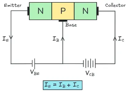
1. Three Terminals of an NPN Transistor
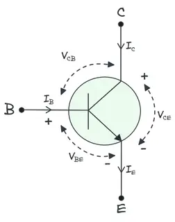
Base (B): Base is the control terminal. A small amount of current flowing into the base controls a larger current flowing through the transistor.
Collector (C): This is the terminal where the main current enters the transistor. The load (an LED, motor, or relay) is connected at the collector side.
Emitter (E): Current exits the transistor through the emitter terminal. The emitter is connected to ground in most of the circuits.
The arrow on the emitter in circuit diagrams shows the direction of conventional current flow. For NPN transistors, the arrow points away from the base.
2. How Does an NPN Transistor Work?
The NPN transistor operates using two junctions, the base-emitter junction and the base-collector junction.
As discussed above, a small amount of current flowing from the base to the emitter allows a larger current to flow from the collector to the emitter. Removing or switching off the base current shuts the collector-emitter path off and no current flows in the collector-emitter path.
For the transistor to turn on:
- The base-emitter voltage \((V_{BE})\) must be approximately 0.6V to 0.7V for silicon transistors.
- The base must be at a higher voltage than the emitter.
- The collector must be at a higher voltage than the emitter.
If \(V_{BE}\) drops below this threshold, the transistor stays off and no collector current flows.
The fundamental point is that the base-emitter junction behaves like a PN junction diode. This junction needs to be forward-biased to get the transistor working.
3. Current Gain (Beta / hFE)
Current gain, called Beta \(\beta\) or \(h_{FE}\) is one of the important characteristics of an NPN transistor.
The value of Beta is responsible for how much the transistor amplifies the base current:
\(I_C=\beta \times I_B\)
Where:
- \(I_C\) = Collector current
- \(I_B\) = Base current
- \(\beta\) = Current gain
For example, if a transistor has a beta of 100 and the supplies base current is 1mA, the collector current will be 100mA.
Beta values range from 20 to 500 depending on the transistor model. You can find the exact beta value in the transistor’s datasheet.
4. Operating Regions of an NPN Transistor
4.1 Cutoff Region
In this region, both the base-emitter and base-collector junctions are reverse-biased. No current flows through the transistor. The transistor is off like an open switch.
In the cutoff region the value of \(V_{BE}\) is less than 0.6V.
4.2 Active Region
In the active region, the base-emitter junction is forward-biased and the base-collector junction is reverse-biased. The transistor is in on state and amplifying in this region.
The collector current is proportional to the base current through the beta relationship. This region is used in amplifier circuits.
4.3 Saturation Region
Both the base-emitter and base-collector junctions are forward-biased. The transistor is fully on like a closed switch. The collector-emitter voltage \((V_{CE})\) drops to a very low value (around 0.2V).
In saturation region, increasing the base current further doesn’t increase the collector current as the transistor is saturated. This region is used in switching circuits for turning loads on and off.
5. NPN Transistor as a Switch
One of the most common uses of an NPN transistor is as a switch. Here’s a simple and practical example to understand the switching procedure of a NPN Transistor.
Suppose, you want to turn on an LED using a microcontroller pin (like an Arduino). The Arduino output is 5V and can supply only about 40mA max. But the load requires 200mA. Then you can use an NPN transistor as a switch.
Circuit Connection and Setup:
- Connect the load (LED) between the positive supply and the collector.
- Connect the emitter to ground.
- Connect the Arduino output pin to the base through a base resistor.
How the Circuit Works:
- Arduino pin goes HIGH → base gets ~5V → V_BE exceeds 0.7V → transistor turns on → current flows through collector → load activates.
- Arduino pin goes LOW → V_BE drops → transistor turns off → load deactivates.
How to Choose Base Resistor:
The load requires 200mA and the transistor has a beta of 100. The minimum base current needed is:
\(I_B = \dfrac{I_C}{\beta} = \dfrac{200mA}{100} = 2mA\)
For saturation, the base current should be 2–10x. If driving 10mA of base current:
\(R_{base} = \dfrac{(V_{in} – V_{BE})}{I_B} = \dfrac{(5V – 0.7V)}{10mA} = 430 \text{ ohms}\)
A standard 470-ohm resistor works here.
6. NPN Transistor as an Amplifier
In the active region, an NPN transistors amplify signals. Due to this property it is used in audio amplifiers, RF circuits, and sensor interfaces.
Common emitter configuration is the most widely used amplifier setup:
- Input signal is applied at the base through a coupling capacitor.
- Output is taken from the collector through another coupling capacitor.
- The emitter is connected to ground (or through a small resistor for stability).
This configuration gives voltage gain and inverts the signal (180° phase shift).
A microphone produces a signal in the microvolt to millivolt range. A common emitter amplifier using an NPN transistor can boost this signal enough to drive a speaker or be processed further.
The voltage gain depends on the collector resistor and the transistor’s transconductance. It can be calculated as:
\(A_v = \dfrac{-RC}{r_e}\)
Where \(r_e = 26mV / IC\) (the transistor’s internal emitter resistance at room temperature).
7. NPN vs PNP Transistors
| Parameter | NPN Transistor | PNP Transistor |
|---|---|---|
| Internal Structure | N-type → P-type → N-type | P-type → N-type → P-type |
| Majority Carriers | Electrons | Holes |
| Turn-On Condition | Base voltage higher than Emitter | Base voltage lower than Emitter |
| Base-Emitter Voltage (V_BE) | Positive (+0.6V to +0.7V) | Negative (-0.6V to -0.7V) |
| Conventional Current Direction | Collector to Emitter | Emitter to Collector |
| Base Current Direction | Flows into the Base | Flows out of the Base |
| Emitter Arrow Direction (Symbol) | Points away from Base | Points toward Base |
| Switching Speed | Faster (electrons move quicker than holes) | Slower (holes are majority carriers) |
| Common Examples | 2N2222, BC547, 2N3904, TIP31C | 2N2907, BC557, 2N3906, TIP32C |
| Preferred Use Case | General switching, amplification, digital logic | High-side switching, complementary amplifier stages |
8. Biasing an NPN Transistor
Biasing means setting the transistor’s DC operating point before any signal is applied. This operating point is called the Q-point (Quiescent Point). Getting the Q-point right is important in amplifier design.
If the Q-point is too high or too low in the active region, the output signal will clip — meaning part of the waveform gets cut off. The goal is to place the Q-point roughly in the middle of the active region so the transistor can amplify both the positive and negative halves of the input signal cleanly.
There are a few biasing methods used in practice.
8.1 Fixed Bias (Base Bias)
This is the simplest biasing method. A single resistor connects the base directly to the supply voltage.
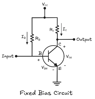
Circuit Connection and Setup:
- \(R_B\) connects from \(V_{CC}\) to the Base.
- \(R_C\) connects from \(V_{CC}\) to the Collector.
- Emitter connects directly to ground.
Formula:
\(I_B = \dfrac{(V_{CC} – V_{BE})}{R_B}\)
The problem with this method is that it depends heavily on beta. If the transistor is replaced with another of the same model number but a different beta value, the Q-point shifts. Temperature changes also affect it. Fixed bias is unstable and rarely used in serious amplifier designs.
8.2 Collector-to-Base Bias (Feedback Bias)
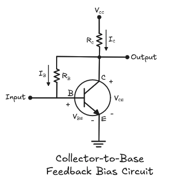
Here, the base resistor connects from the Collector to the Base instead of from \(V_{CC}\) to the Base.
This gives a degree of self-regulation. If the collector current increases, the collector voltage drops. A lower collector voltage means less base current, which then reduces the collector current. This feedback action keeps the Q-point more stable than fixed bias.
It’s still not the most stable method, but it’s better than fixed bias and uses fewer components.
8.3 Voltage Divider Bias
This is the most stable and most commonly used biasing method in amplifier circuits.
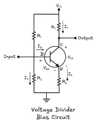
Circuit Connection and Setup:
- \(R_1\) connects from \(V_{CC}\) to the Base.
- \(R_2\) connects from the Base to Ground.
- \(R_1\) and \(R_2\) form a voltage divider that sets the base voltage.
- \(R_C\) connects from \(V_{CC}\) to the Collector.
- \(R_E\) connects from the Emitter to Ground.
The emitter resistor \(R_E\) makes this method more stable. If the collector current increases due to temperature or beta variation, the emitter voltage increases. This reduces \(V_{BE}\) which reduces the base current, which then brings the collector current back down. This is called negative feedback, and it keeps the Q-point steady.
Practical Example:
Suppose \(V_{CC} = 12V\) and you want \(V_{CE} ≈ 6V\) with \(I_C = 5mA\).
Step 1 — Choose RC:
\(R_C = \dfrac{(V_{CC} – V_{CE})}{I_C} = \dfrac{(12V – 6V)}{5mA} = 1.2kΩ\)
Step 2 — Choose RE (5–10% of V_CC):
\(V_{RE} = 1.2V\) (10% of 12V)
\(R_E = \dfrac{V_{RE}}{I_C} = \dfrac{1.2V}{5mA} = 240Ω\) → use 220Ω standard resistor
Step 3 — Find required base voltage:
\(V_B = V_{BE} + V_{RE} = 0.7V + 1.2V = 1.9V\)
Step 4 — Choose R1 and R2 to set V_B = 1.9V:
Use a divider current of about 10× the base current for stability. If beta = 100:
\(I_B = \dfrac{I_C}{\beta }= \dfrac{5mA}{100} = 0.05mA\)
\(\text{Divider current} = 10 \times 0.05mA = 0.5mA\)
\(R_2 = \dfrac{V_B}{I_{divider}} = \dfrac{1.9V}{0.5mA} = 3.8kΩ\) → use 3.9kΩ
\(R_1 = \dfrac{(V_{CC} – V_B)}{I_{divider}} = \dfrac{(12V – 1.9V)}{0.5mA} = 20.2kΩ\) → use 20kΩ
This circuit will hold the Q-point steady even if you swap the transistor or if the temperature rises.
9. Common NPN Transistor Circuit Configurations
There are three fundamental configurations for connecting an NPN transistor in a circuit:
9.1 Common Emitter (CE)
- Emitter is the common terminal between input and output.
- Provides high voltage gain and current gain.
- Input at base, output at collector.
- Output is inverted.
- Most used configuration in amplifier circuits.
9.2 Common Base (CB)
- Base is the common terminal.
- Input at emitter, output at collector.
- Provides voltage gain but no current gain (current gain < 1).
- Good for high-frequency applications due to no Miller effect.
9.3 Common Collector (CC) — Also called Emitter Follower
- Collector is the common terminal.
- Input at base, output at emitter.
- No voltage gain (gain ≈ 1), but good current gain.
- Output follows the input signal closely.
- Used for impedance matching — connecting a high-impedance source to a low-impedance load.
10. Applications of NPN Transistors
NPN transistors appear in almost every category of electronics:
Digital logic circuits: Early logic gates were built using transistors. Even now, the internal structure of CMOS logic gates includes transistors.
Motor drivers: An NPN transistor (or a Darlington pair using two NPN transistors) can switch a motor on and off under microcontroller control. The TIP120 is a popular Darlington NPN transistor for this purpose.
Audio amplifiers: From guitar effects pedals to speaker amplifiers, NPN transistors in common-emitter configuration provide signal amplification.
Relay drivers: Relays need 50–150mA to activate their coil. A microcontroller pin can’t supply that directly. An NPN transistor handles the switching between the microcontroller and the relay.
Oscillators: NPN transistors are used in LC and RC oscillator circuits to generate continuous waveforms.
Signal detection circuits: Infrared receivers, photodiode amplifiers, and temperature sensor circuits often use NPN transistors to boost weak signals from sensors.
11. Darlington Pair
Sometimes a single transistor doesn’t provide enough current gain. A Darlington pair connects two NPN transistors so that the emitter of the first transistor feeds into the base of the second.
The overall gain is:
\(\beta_{total} = \beta_1 \times \beta_2\)
If each transistor has a beta of 100, the combined gain is 10,000. This means a very tiny base current can control a very large collector current.
Darlington transistors are available as pre-made packages (like TIP120, TIP122). They’re common in motor control and high-current relay switching.
12. Conclusion
An NPN transistor is a bipolar junction transistor with two N-type layers sandwiching one P-type base layer. It conducts when the base-emitter voltage reaches 0.6 to 0.7V. A small base current controls a larger collector current through the beta relationship.
NPN transistors operate in cutoff, active, and saturation regions. They are used in switching, amplification, relay driving, and motor control circuits.
13. Frequently Asked Questions (FAQs)
NPN stands for Negative-Positive-Negative. It describes the three layers of semiconductor material inside the transistor: two N-type (electron-rich) layers with one P-type (hole-rich) layer in between.
A silicon NPN transistor requires approximately 0.6V to 0.7V across the base-emitter junction (V_BE) to turn on.
No. NPN transistors are designed for DC circuits. To control AC loads, you need components like TRIACs, SCRs (thyristors), or solid-state relays.
Most NPN transistors will not work properly in reverse. The transistor has an inverse active mode where it can conduct slightly, but the gain is very low and the transistor may be damaged depending on the voltages applied.
No. Beta varies with collector current, temperature, and even from one transistor to another of the same model number.
Both are used for switching and amplification, but they work differently. A BJT (like an NPN transistor) is a current-controlled device. A small base current controls the collector current. A MOSFET is a voltage-controlled device. A gate voltage controls the drain current, and theoretically no gate current is needed.
Not directly in most circuits. A PNP transistor has specific behavior that depends on its structure. You can sometimes use an NPN transistor with additional components to replicate the function of a PNP in certain switching configurations, but it’s usually simpler to just use the correct transistor type for the job.