
A Zener diode is a two-terminal semiconductor device made from heavily doped P-type and N-type silicon semiconductors. Zener diode operates in the reverse-biased condition and it maintains constant voltage across its terminals when the applied voltage reaches a specific value. This specific voltage at which Zener diode maintains constant voltage is called the Zener breakdown voltage or Zener voltage \((V_z)\).
Zener diodes are available in a wide range of Zener voltages from 1.8V to several hundred volts. Common values Zener voltages used regularly include 3.3V, 5.1V, 6.8V, 12V, and 15V.
1. Symbol of a Zener Diode
The symbol of a Zener diode is similar to a regular PN junction diode. It has an anode and a cathode. The only difference is that the cathode end has small bent edges (like the letter Z) on the vertical bar as shown in the figure below.
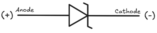
This bent symbol is a visual representation to remind that the device is designed for the reverse breakdown region. In circuit diagrams, the cathode is always connected toward the positive supply when the diode is reverse biased.
2. Construction of a Zener Diode
A Zener diode is constructed using heavily doped P-N junction semiconductor material as mentioned above. Silicon is the most common semiconductor material used for construction of Zener diode because it can handle higher temperatures compared to germanium.
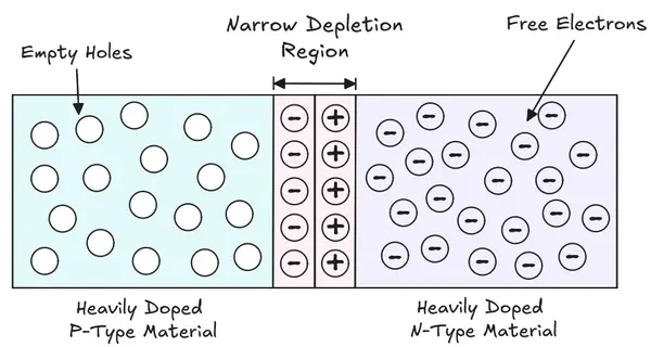
The heavy doping on both P-side and N-sides of the junction creates a very narrow depletion region as shown in the figure above. This narrow depletion region means that the electric field across the depletion region is very strong. The strong electric field causes the Zener breakdown to occur at a predetermined and stable voltage level.
The doping concentration directly impacts the breakdown voltage. Higher doping gives a lower Zener breakdown voltage. Lower doping gives a higher Zener breakdown voltage.
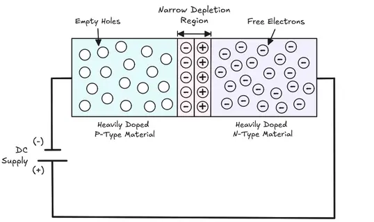
3. Working Principle of a Zener Diode
3.1 Forward Bias Operation
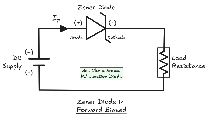
In forward bias, a Zener diode works just like an ordinary P-N junction diode. The anode is connected to the positive terminal and the cathode is connected to the negative terminal as shown in the figure above. When the forward voltage crosses approximately 0.7 V (for silicon constructed Zener diodes), the diode conducts normally and the current \(I_z\) flows through the circuit.
Zener diodes are generally not used in forward biased condition in most of the circuits.
3.2 Reverse Bias Operation
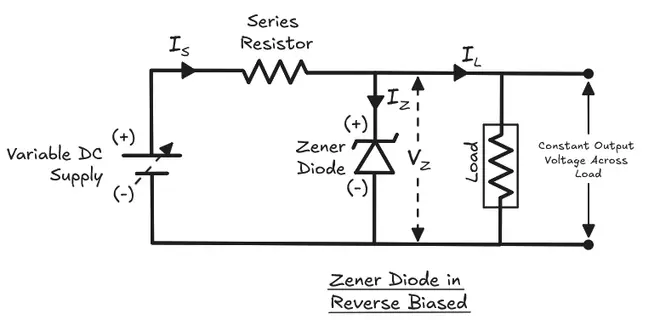
When the Zener diode is reverse biased, initially a small amount of reverse leakage current flows. If the reverse voltage is increased to a specific value, the current suddenly increases rapidly. This point is the Zener breakdown voltage.
After the Zener breakdown voltage, even if the current increases rapidly, the voltage across the Zener diode remains almost constant \((V_z)\). The diode clamps the voltage at the Zener voltage.
This fundamental property makes Zener diodes useful in voltage regulation.
4. Zener Breakdown vs. Avalanche Breakdown
There are two mechanisms that causes reverse breakdown in a diode. These are called Zener breakdown and avalanche breakdown.
4.1 Zener Breakdown
Zener breakdown occurs in heavily doped diodes with a thin depletion layer. The strong electric field in the depletion region pulls electrons directly from their covalent bonds. This process is called quantum tunneling or the Zener effect. It does not require any high-energy collisions.
Zener breakdown occurs at voltages below 5.5V.
4.2 Avalanche Breakdown
Avalanche breakdown occurs in lightly doped diodes with a wider depletion region. Free electrons gain enough energy from the electric field to knock other electrons loose through collisions. Those new electrons knock even more electrons loose and creates a chain reaction.
Avalanche breakdown occurs at voltages above 5.5V.
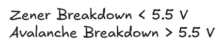
Both the Zener breakdown and Avalanche Breakdown are controlled and reversible. The device returns to normal when the voltage drops below the breakdown level.
5. V-I Characteristics of a Zener Diode
5.1 Forward Characteristics
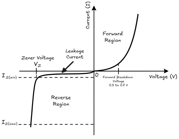
In forward bias, the curve is identical to a regular PN junction diode. Current starts flowing after the forward voltage crosses 0.7V. Beyond the forward breakdown voltage the current rises steeply.
5.2 Reverse Characteristics
In reverse bias, a small reverse leakage current (called reverse saturation current) flows as the reverse voltage is slowly increased. This current is negligible.
At the Zener voltage \((V_z)\), the curve shows a sharp bend. The voltage stays nearly flat at \(V_z\) regardless of increase in current. This flat portion of the reverse curve is the regulation region. Zener diode is operated in this regulation region for voltage regulation purposes.
5.3 Knee of the Curve
The point where the reverse current sharply increases is called the knee of the V-I curve. The Zener voltage \((V_z)\) is measured at the knee point.
6. Parameters of a Zener Diode
6.1 Zener Voltage (Vz)
As discussed in the above sections, this is the nominal reverse breakdown voltage. For example, a 5.1V Zener diode will maintain approximately 5.1V across its terminals when operating in the breakdown region.
6.2 Zener Current (Iz)
This is the reverse current through the diode at the rated Zener voltage. It includes:
- \(I_{zk}\) (knee current): the minimum current needed to enter the regulation region
- \(I_{zt}\) (test current): the current at which \(V_z\) is measured (usually listed in datasheets)
- \(I_{zm}\) (maximum current): maximum allowable reverse current before the diode is damaged
6.3 Power Dissipation (Pz)
Power dissipation is the maximum power the diode can handle. It is calculated as:
\(P_z = V_z \times I_z\)
For example, a 5.1V Zener with 20mA of current dissipates 102mW.
Common power ratings are 400mW, 500mW, 1W, 5W, and 10W.
6.4 Zener Impedance (Zz)
In an ideal Zener diode, the voltage is perfectly constant in the breakdown region. In reality, the Zener voltage changes slightly with current. Zener impedance tells how much the Zener voltage changes with current. A lower Zener impedance \((Z_z)\) means better and stable voltage regulation.
6.5 Temperature Coefficient
The Zener voltage changes with temperature. This change is expressed as mV/°C. Diodes with \(V_z\) below 5V have a negative temperature coefficient. Diodes with \(V_z\) above 6V have a positive coefficient.
Around 5V to 6V, the temperature coefficient is close to zero.
7. Zener Diode as a Voltage Regulator
The most common application of a Zener diode is as a shunt voltage regulator. This circuit maintains a constant output voltage regardless of variations in the supply voltage or the load current.
7.1 Circuit Diagram
A Zener diode is connected in reverse bias across the output (load). A series resistor \((R_s)\) is placed between the supply voltage \((V_{in})\) and the Zener diode to limit current.
The output voltage is taken across the Zener diode, which is also across the load \((R_L)\).
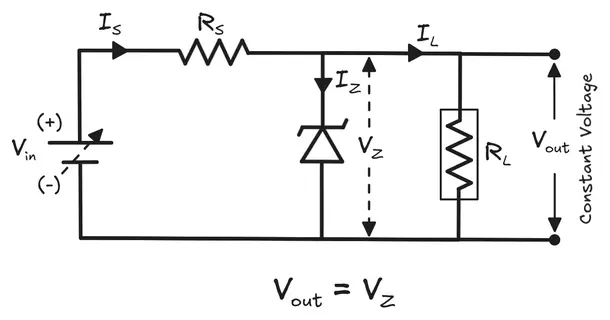
When the input voltage increases the Zener diode absorbs excess current. The voltage across the diode stays constant at \(V_z\) and hence the load receives a constant voltage.
If the load current increases, the Zener current decreases to compensate this increase in load current and keeps \(V_{out}\) constant.
7.2 Practical Example
Suppose,
\(V_{in} = 12V\),
\(V_z = 5.1V\), and
\(R_s = 470\Omega\).
Current through \(R_s = \dfrac{(12 – 5.1)}{470} = \dfrac{6.9}{470} ≈ 14.7\text{ mA}\)
If the load draws 5mA, the Zener takes the remaining 9.7mA. The output stays at 5.1V.
8. How to Calculate the Value of Series Resistor?
The formula for calculating the desired value of series resistor is:
\(R_s = \dfrac{(V_{in} – V_z)}{(I_z + I_L)}\)
Where:
- \(V_{in}\) = input supply voltage
- \(V_z\) = Zener voltage
- \(I_z\) = desired Zener current
- \(I_L\) = load current
Power rating of \(R_s\):
\(P(R_s) = \dfrac{{(V_{in} – V_z)}^2}{R_s}\)
9. Zener Diode for Overvoltage Protection
A Zener diode placed across a load acts as a voltage clamp. If the supply voltage suddenly spikes above \(V_z\), the Zener conducts and clamps the voltage at \(V_z\). This action of a Zener diode protects the load.
Example: A microcontroller input pin rated at 5V max needs protection. A 5.1V Zener placed from the signal line to GND will clamp any voltage spike above 5.1V and prevents damage to the input pin.
This configuration is simple, fast-acting, and inexpensive.
10. Zener Diode as a Waveform Clipper
Zener diodes can clip portions of an AC waveform.
If two Zener diodes are connected back-to-back (anode to anode or cathode to cathode) in a circuit, the positive half cycle is clipped at \(V_z + 0.7V\) and the negative half cycle is also clipped at the same level.
This produces a square-wave-like output from a sine wave input. This is used in waveform shaping and simple signal conditioning circuits.
11. Common Zener Diode Series and Part Numbers
Here are some widely used Zener diodes you will come across in practical circuits:
| Part Number | Zener Voltage | Power Rating |
|---|---|---|
| 1N4728A | 3.3V | 1W |
| 1N4733A | 5.1V | 1W |
| 1N4739A | 9.1V | 1W |
| 1N4742A | 12V | 1W |
| 1N4744A | 15V | 1W |
| BZX55C5V1 | 5.1V | 500mW |
| BZX79C12 | 12V | 500mW |
12. Difference Between Zener Diode and Regular Diode
| Feature | Regular Diode | Zener Diode |
|---|---|---|
| Reverse Bias | Blocks current | Conducts at \(V_z\) |
| Breakdown | Destroys diode | Controlled, reversible |
| Main Use | Rectification | Voltage regulation |
| Doping | Lighter | Heavier |
13. Conclusion
A Zener diode is a reverse-biased semiconductor device that maintains a fixed voltage across its terminals after reaching its breakdown voltage.
Its main applications are in voltage regulation, voltage reference generation, overvoltage protection, and waveform clipping.
Zener diodes are inexpensive and easy to use. They remain one of the most practical components in analog circuit design.
14. Frequently Asked Questions (FAQs)
The Zener voltage is the specific reverse breakdown voltage at which the Zener diode starts conducting and maintains a nearly constant voltage. It is a fixed value set during manufacturing through controlled doping. Common values are 3.3V, 5.1V, 9.1V, and 12V.
Yes, a Zener diode conducts in forward bias just like a regular silicon diode with a forward voltage drop of approximately 0.7V. However, its useful and intended operating region is reverse bias at the Zener breakdown voltage.
If the current exceeds the maximum rated Zener current (Izm), the power dissipation will exceed the diode’s rating. This causes excessive heating and permanently damages the diode.
Zener breakdown occurs due to quantum tunneling through a narrow depletion layer in heavily doped diodes at voltages below 5.5V. Avalanche breakdown occurs due to impact ionization in lightly doped diodes at voltages above 5.5V. Both are reversible.
Without a series resistor, the current through the Zener is limited only by the source impedance. Excessive current will destroy the diode. The series resistor limits the current and drops the excess voltage between the supply and Vz.
Yes. Zener diodes can be connected in series to achieve a higher combined Zener voltage. For example, two 6V Zener diodes in series give a 12V regulation voltage. The current through both diodes is the same, but the total voltage drop is the sum of both Zener voltages.