
A Bipolar Junction Transistor (BJT) is a three-terminal semiconductor device. It is constructed by sandwiching three alternating layers of P-type and N-type semiconductor materials. Based on the arrangement of semiconductor layers, a Bipolar Junction Transistor can be divided into NPN or PNP types.
As shown in the figure below, a Bipolar Junction Transistor has three terminals known as the emitter, base, and collector. A BJT is called bipolar because it uses both electrons and holes as charge carriers.
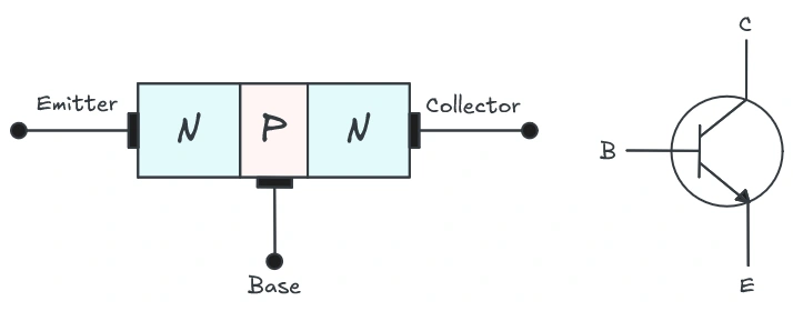
A small input current applied to the thin base region controls a larger current flowing between the emitter and collector. Because of this, BJTs are highly effective for signal amplification and electronic switching applications in various circuits.
1. Types of BJT
1.1 NPN Transistor
In an NPN transistor, a thin P-type layer is sandwiched between two N-type layers. The majority charge carriers in an NPN transistor are electrons. Current flows from the collector to the emitter, but electrons move from the emitter to the collector.
The base-emitter junction in an NPN transistor is forward biased and the base-collector junction is reverse biased. This allows the transistor to effectively amplify or switch signals.
A common example of an NPN transistor is the 2N2222, widely used in low-power switching and amplification applications because of its reliable performance and availability.
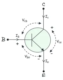
The circuit symbol of an NPN transistor shows the arrow points away from the base as shown in the figure below. This shows the direction of conventional current flow through the emitter.
This outward arrow also helps distinguish the NPN transistor from its PNP counterpart.
1.2 PNP Transistor
In a PNP transistor, a thin N-type layer is sandwiched between two P-type layers. The majority charge carriers in a PNP transistor are holes. In a PNP transistor, current flows from the emitter to the collector which is opposite to the current flow in an NPN transistor.
The base-emitter junction in a PNP transistor is forward biased, while the base-collector junction is reverse biased to control and amplify electrical signals.
A common example of a PNP transistor is the 2N3906. This transistor is widely used in low-power switching and amplification applications paired with NPN transistors in complementary circuit designs.
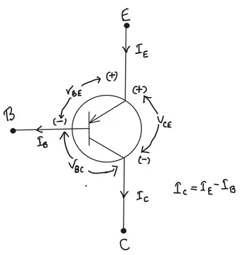
The circuit symbol of a PNP transistor shows the arrow pointing toward the base as shown in the figure below. This indicates the direction of conventional current flow through the emitter.
2. Physical Structure of a BJT
As discussed above, a BJT has three semiconductor regions with different doping levels and physical sizes as shown in the figure below. Each region plays a distinct role in the overall operation of the transistor.
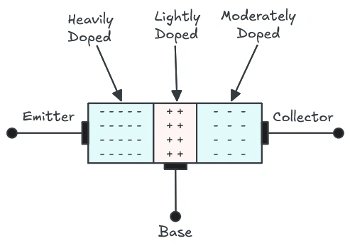
The emitter is heavily doped. The job of the emitter is to inject a large number of charge carriers into the base region. As shown in the figure, the emitter region contains a high concentration of negative charge carriers or electrons in the NPN configuration.
The base is very thin and lightly doped. A thin base allows most of the carriers injected from the emitter to pass through and reach the collector without recombining.
The collector is moderately doped and physically larger than the emitter. It collects the carriers that successfully cross the base region. The larger physical size of the collector allows it to gather and dissipate the heat generated during the collection of charge carriers.
The current gain and overall performance of a transistor directly depends upon the doping levels and physical dimensions of these three regions.
3. How Does a BJT Work?
A BJT has two junctions: Emitter-Base Junction (EBJ) and Collector-Base Junction (CBJ). The operation of a BJT depends on the biasing of these two junctions.
3.1 Active Mode Operation (Most Common)
In the active mode, the emitter-base junction is forward biased and the collector-base junction is reverse biased.
Step 1: Carrier Injection at the Emitter-Base Junction
The forward bias applied at the emitter-base junction reduces the potential barrier between the emitter and the base. This allows electrons from the heavily doped emitter to cross into the base region. Because the emitter is heavily doped, a large number of electrons are available for injection.
Step 2: Carrier Transport Through the Base
The base is very thin and lightly doped. Once electrons enter the base, they encounter very few holes to recombine with. The majority of these electrons diffuse through the base region without recombining. Only a tiny fraction recombines with holes in the base. That recombination current forms the base current \((I_B)\).
Step 3: Carrier Collection at the Collector
The reverse bias at the collector-base junction creates a strong electric field at that junction. As electrons reach the collector-base junction, this electric field sweeps them directly into the collector. This forms the collector current \((I_C)\).
Step 4: Current Relationship
Since most electrons injected by the emitter reach the collector, \(I_C\) is much larger than \(I_B\). A small change in base current produces a proportionally large change in collector current. This relationship is expressed as:
\(I_C = \beta \times I_B\)
Where \(\beta\) is the DC current gain of the transistor. For most small-signal BJTs, \(\beta\) ranges from 50 to 500.
3.2 Practical Example
Take an NPN transistor with β = 150. A base current of 40 µA is applied. The resulting collector current is:
\(I_C = 150 \times 40 µA = 6 mA\)
A 40 µA signal at the base controls a 6 mA current at the collector. This is the amplification action of the BJT in active mode.
It is also worth noting that the emitter current \((I_E)\) is the sum of the base current and the collector current:
\(I_E = I_B + I_C\)
This follows directly from Kirchhoff’s Current Law (KCL) applied at the transistor terminals.
4. BJT Operating Modes
A BJT operates in four different modes depending on how its two junctions are biased. Each mode produces a different behavior at the output.
Here is a summary table before going into the details:
| Operating Mode | EBJ Bias | CBJ Bias | Used For |
|---|---|---|---|
| Active | Forward | Reverse | Amplification |
| Saturation | Forward | Forward | Switch ON |
| Cut-off | Reverse | Reverse | Switch OFF |
| Inverse Active | Reverse | Forward | Rarely used |
4.1 Active Mode
As discussed above, the emitter-base junction is forward biased and the collector-base junction is reverse biased in active mode.
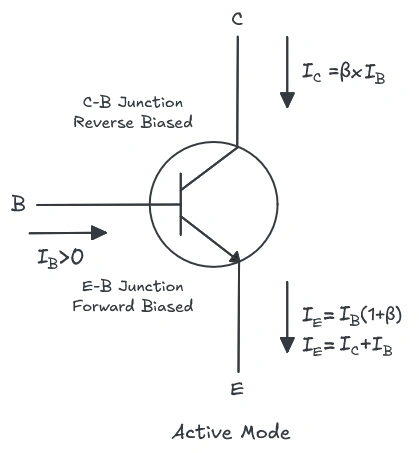
This mode is used for signal amplification. The transistor acts as a current-controlled current source. A small base current \((I_B)\) controls a larger collector current \((I_C)\).
The relationship is: \(I_C = \beta \times I_B\)
In this mode, the collector current is independent of the collector-emitter voltage \((V_{CE})\) as long as \(V_{CE}\) stays above a minimum threshold. Below this voltage, the transistor starts entering saturation.
4.2 Saturation Mode
In saturation mode, both the emitter-base junction and the collector-base junction are forward biased.
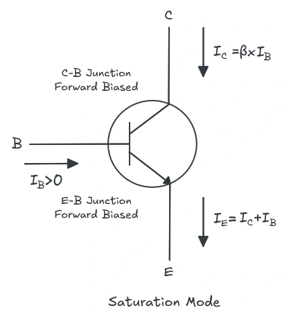
The transistor is fully ON in this mode. It conducts heavily and the voltage across the collector and emitter \((V_{CE})\) drops to a very small value. For silicon transistors, \(V_{CE(sat)}\) is around 0.1V to 0.3V.
In saturation, the collector current is no longer controlled by the base current through the \(\beta\) relationship. It is determined by the supply voltage and the collector resistor. The transistor simply provides a low-resistance path between the collector and emitter.
The condition for saturation is:
\(I_B ≥ \dfrac{I_{C(sat)}}{\beta}\)
If the base current is supplied more than this minimum value, the transistor goes deeper into saturation.
Practical Example:
In a relay driver circuit, an NPN transistor is driven into saturation to energize the relay coil. The collector is connected to one end of the relay coil and the other end goes to \(V_{CC}\). A sufficient base current is supplied so that the transistor saturates and the full supply voltage appears across the relay coil.
Suppose \(V_{CC} = 12V\), relay coil resistance = 120Ω, and \(\beta = 100\).
- \(I_{C(sat)} = \dfrac{12V}{120Ω} = 100 mA\)
- Minimum \(I_B\) required = \dfrac{100 mA}{100} = 1 mA\)
- With an overdrive factor of 5: \(I_B = 5 mA\)
So the base resistor must be chosen to supply at least 5 mA of base current.
4.3 Cut-off Mode
In cut-off mode, both the emitter-base junction and the collector-base junction are reverse biased.
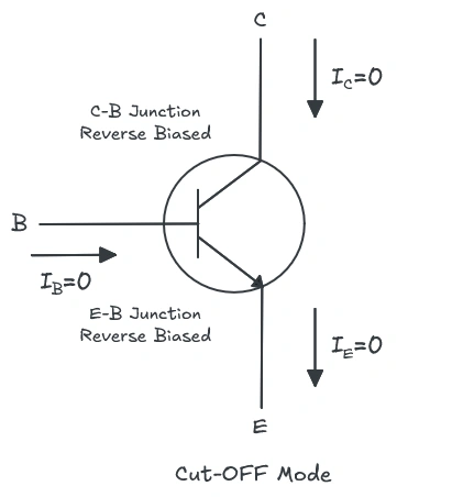
The transistor is fully OFF in this mode. No current flows between the collector and emitter. Only a very small leakage current flows in the nanoampere range and can be ignored.
The transistor behaves like an open switch between the collector and emitter terminals.
For an NPN transistor to enter cut-off, the base-emitter voltage \((V_{BE})\) must be below the threshold voltage. For silicon BJTs, this means \(V_{BE}\) must be less than approximately 0.5V. In most digital circuits, applying 0V to the base is enough to cut off the transistor.
4.4 Inverse Active Mode
In inverse active mode, the emitter-base junction is reverse biased and the collector-base junction is forward biased. This is the opposite of the normal active mode.
The transistor does conduct in this mode, but the current gain is very low. This happens because the collector is not designed for carrier injection. The collector is moderately doped, so it cannot inject as many carriers as the heavily doped emitter can.
The inverse current gain \((\beta_R)\) is much lower than the forward current gain \((\beta_F)\). For most transistors, \(\beta_R\) is in the range of 0.1 to 5.
5. BJT as a Switch
A BJT can work as an electronic switch in digital circuits. It toggles between cut-off (OFF) and saturation (ON).
Consider a simple LED driver using an NPN BJT as shown in the figure below:
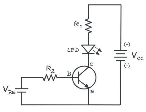
- The LED and a resistor are connected from the supply voltage \((V_{CC})\) to the collector.
- The emitter is connected to ground.
- A resistor is placed in series with the base.
When the input voltage at the base is HIGH (logic 1), the transistor enters saturation. Current flows through the LED and it lights up.
When the input voltage is LOW (logic 0), the transistor enters cut-off. No current flows and the LED turns off.
To make sure the transistor is in saturation, you need to provide enough base current. The condition for saturation is:
\(I_B ≥ \dfrac{I_{C(sat)}}{\beta}\)
If the LED requires 10 mA and \(\beta = 100\), you need at least 0.1 mA of base current.
6. BJT as an Amplifier
A BJT amplifier takes a weak input signal and produces a stronger output signal. The basic idea is that a small change in base current causes a proportional large change in collector current.
There are three standard amplifier configurations for a BJT:
6.1 Common Emitter (CE) Configuration
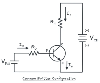
The emitter terminal is common to both the input and output. This is the most frequently used amplifier configuration.
- High voltage gain
- High current gain
- 180° phase inversion between input and output
Practical Example: Audio preamplifiers often use the common emitter configuration because it provides strong voltage amplification.
6.2 Common Base (CB) Configuration
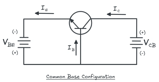
The base terminal is common to both the input and output.
- High voltage gain
- Current gain less than 1
- No phase inversion
- Good high-frequency performance
The common base configuration is used in RF and high-frequency circuits because of its good bandwidth characteristics.
6.3 Common Collector (CC) Configuration (Emitter Follower)
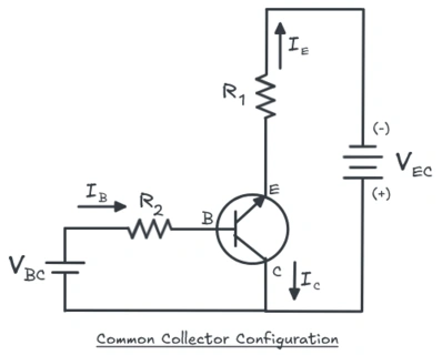
The collector is common to both the input and output. The output is taken from the emitter.
- Voltage gain is approximately 1
- High current gain
- No phase inversion
- Low output impedance
This configuration is used as a buffer to match impedance between stages. For example, if you want to connect a high-impedance microphone to a low-impedance speaker, an emitter follower helps transfer the signal without loss.
7. BJT Biasing Techniques
To operate a BJT in the active region for amplification, you must establish a stable DC operating point, called the Q-point (quiescent point). Biasing circuits set this operating point.
7.1 Fixed Bias (Base Bias)
A single resistor connects the base to the supply voltage. It is simple but provides poor stability. If the transistor is replaced or if temperature changes, the Q-point shifts.
7.2 Emitter Bias (Two-Supply Bias)
Uses two power supplies: one positive and one negative. The emitter is connected to the negative supply through a resistor. This gives good stability.
7.3 Voltage Divider Bias
This is the most stable and commonly used biasing method. Two resistors (R1 and R2) form a voltage divider that sets the base voltage. An emitter resistor provides additional stability through negative feedback.
7.4 Collector-to-Base Bias
A feedback resistor connects the collector to the base. If \(I_C\) increases, the collector voltage drops. This reduces the base current, which reduces \(I_C\). It provides moderate stability.
8. Practical Applications of BJT
1. Audio Amplifiers: The common emitter amplifier configuration is used in the preamplifier stage of audio systems to amplify weak microphone signals.
2. Radio Frequency Amplifiers: High-frequency BJTs like the BFR93 are used in RF front-end circuits to amplify received signals in mobile phones and radios.
3. Switching Regulators: BJTs serve as switches in older power supply designs. The transistor switches ON and OFF rapidly to control output voltage.
4. Current Sources: BJTs are used to build stable current sources. A common example is the Widlar current mirror, found in operational amplifier (op-amp) ICs.
5. Darlington Pair: Two BJTs are connected together to form a Darlington pair. The combined current gain is β1 × β2. This gives a very high input impedance and is used in applications like touch-sensitive circuits and power amplifiers.
6. Logic Gates: Early transistor-transistor logic (TTL) gates used BJTs. TTL ICs like the 7400 series use BJTs internally.
7. Temperature Sensor: V_BE of a BJT changes predictably with temperature (about -2 mV/°C). This property is used in temperature measurement circuits and bandgap voltage references.
9. Conclusion
The Bipolar Junction Transistor is a fundamental building block in analog and digital electronics. From simple LED switching circuits to complex RF amplifiers, the BJT serves across a wide range of applications. It operates through precise control of two P-N junctions, two charge carriers, and defined biasing conditions as discussed above.
10. Frequently Asked Questions (FAQs)
The term “bipolar” means that both types of charge carriers, electrons and holes, participate in current conduction. This is different from a unipolar device like a MOSFET, where only one type of carrier (either electrons or holes) conducts.
In an NPN transistor, the base is P-type and the emitter/collector are N-type. Electrons are the majority carriers. In a PNP transistor, the base is N-type and the emitter/collector are P-type. Holes are the majority carriers.
Beta (β) is the DC current gain of a BJT. It is the ratio of collector current to base current: β = I_C / I_B. For small-signal transistors, β typically ranges from 50 to 500. For the popular 2N2222, β is between 100 and 300.
In active mode, the emitter-base junction is forward biased and the collector-base junction is reverse biased. The transistor amplifies signals in this mode. In saturation mode, both junctions are forward biased. The transistor acts like a closed switch and V_CE drops to a very low value.
The emitter is heavily doped to inject a large number of charge carriers into the base region. A higher carrier concentration in the emitter means more carriers are available to flow toward the collector, which improves the current gain of the transistor.
V_BE is the base-to-emitter voltage. It is the forward voltage drop across the emitter-base junction. For silicon BJTs, V_BE is approximately 0.6V to 0.7V.